


Environmental, bioanalytical and diagnostic sensor technology combined with smart microfluidic lab-on-a-chip and organ-on-a-chip systems
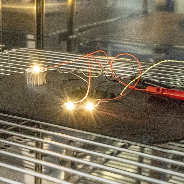
Cost-effective solutions by extending the functions of classic LED-based lighting systems in the areas of Visible Light Communication, Visible Light Positioning and Visible Light Sensing
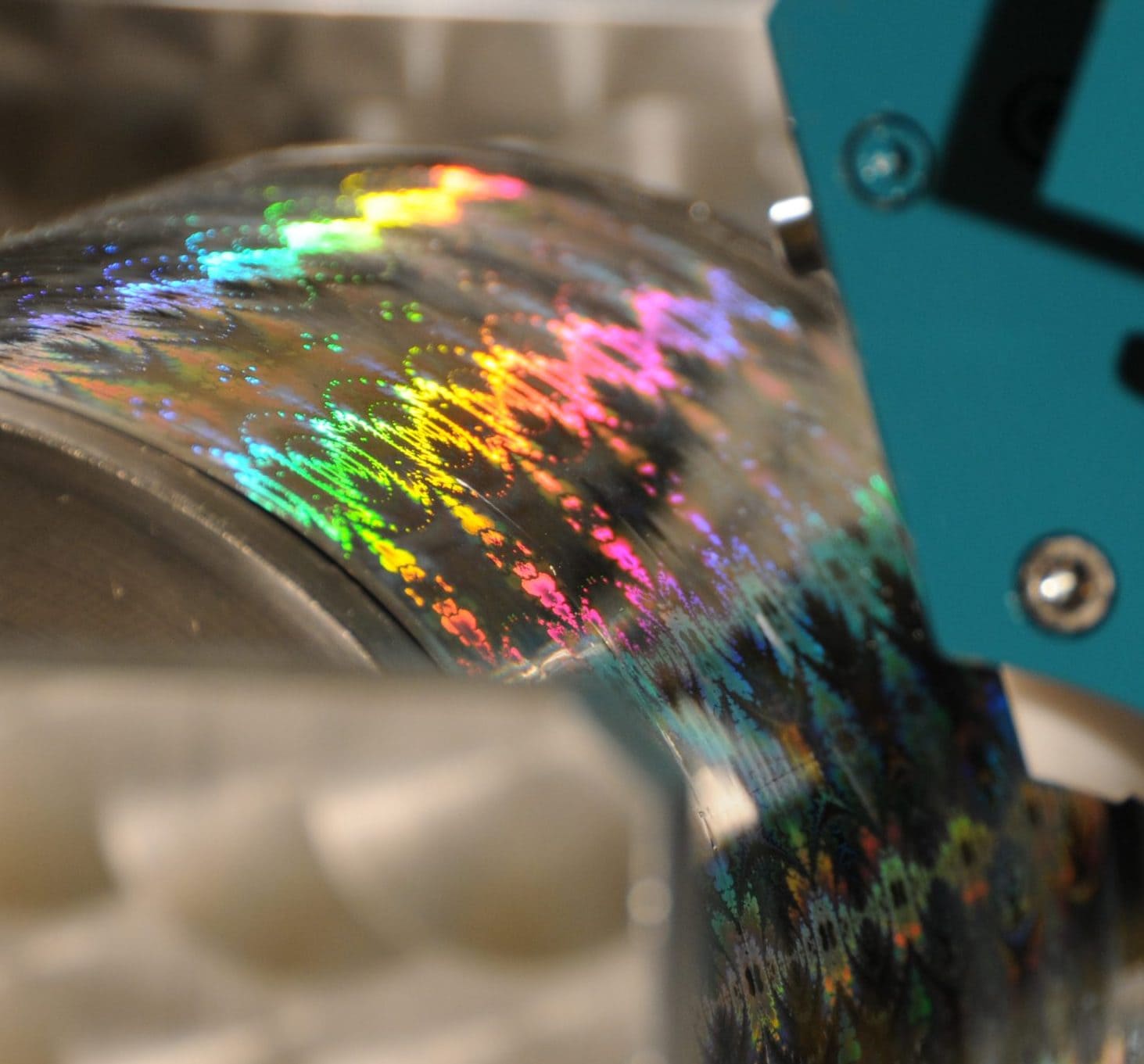
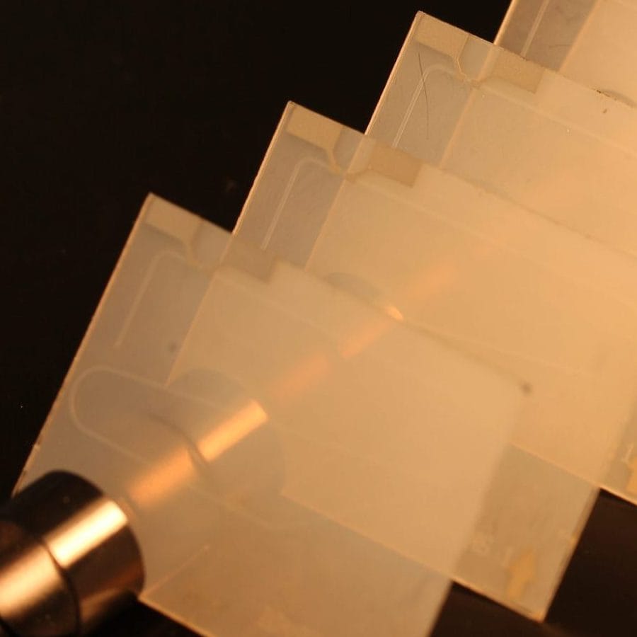
R2R-UV-NIL pilot line for the continuous and cost-effective production of micro- and nanostructures on flexible large-area film substrates
Replication of master structures almost seamlessly onto large surfaces (380 x 700 mm²) using a step&repeat UV-NIL process
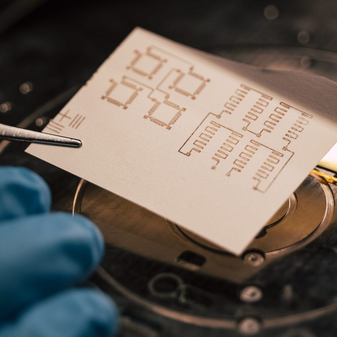
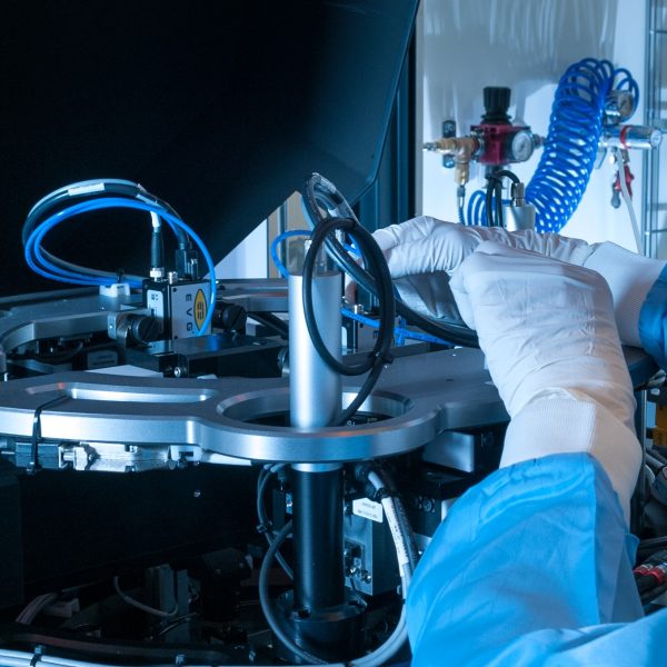
Measurement and analysis of the smallest structures, layers and components on a micro- and nanometre scale
Technology for extending the pot life of silicones to several months without changing the material properties
Complete solutions from optical simulation, mastering and prototyping to the transition to high volume, cost effective production of optical structures and components
Reusable materials, components and compounds and their applications, e,g, coatings developed in-house for UV imprint lithography (NILcure®)
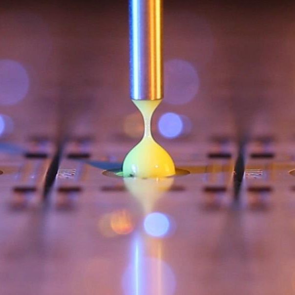
Printable sensor inks and sensors with piezoelectric, pyroelectric and magnetoelectric features
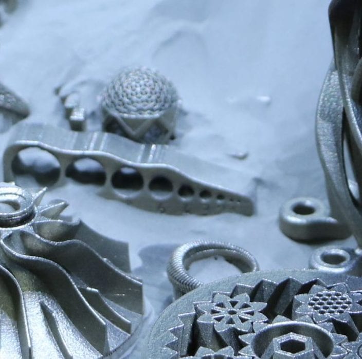
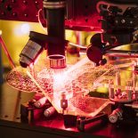
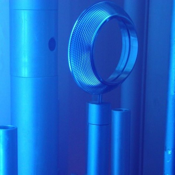
Additive manufacturing thanks to new design and simulation tools, new materials and the realisation of special topological structures
Functional coating processes: Plasma and vacuum coating (PVD, PA-CVD), atmospheric pressure plasma coating processes as well as digital printing processes