Our services include the development, characterisation and production of functional coatings under atmospheric pressure (~1013 hPa (mbar)), in low pressure fine vacuum (~0.1 Pa) and high vacuum (~10-5 Pa) and range from problem analyses, literature research and feasibility studies to prototype production and small series coating.
What is an atmospheric pressure plasma coating system for?
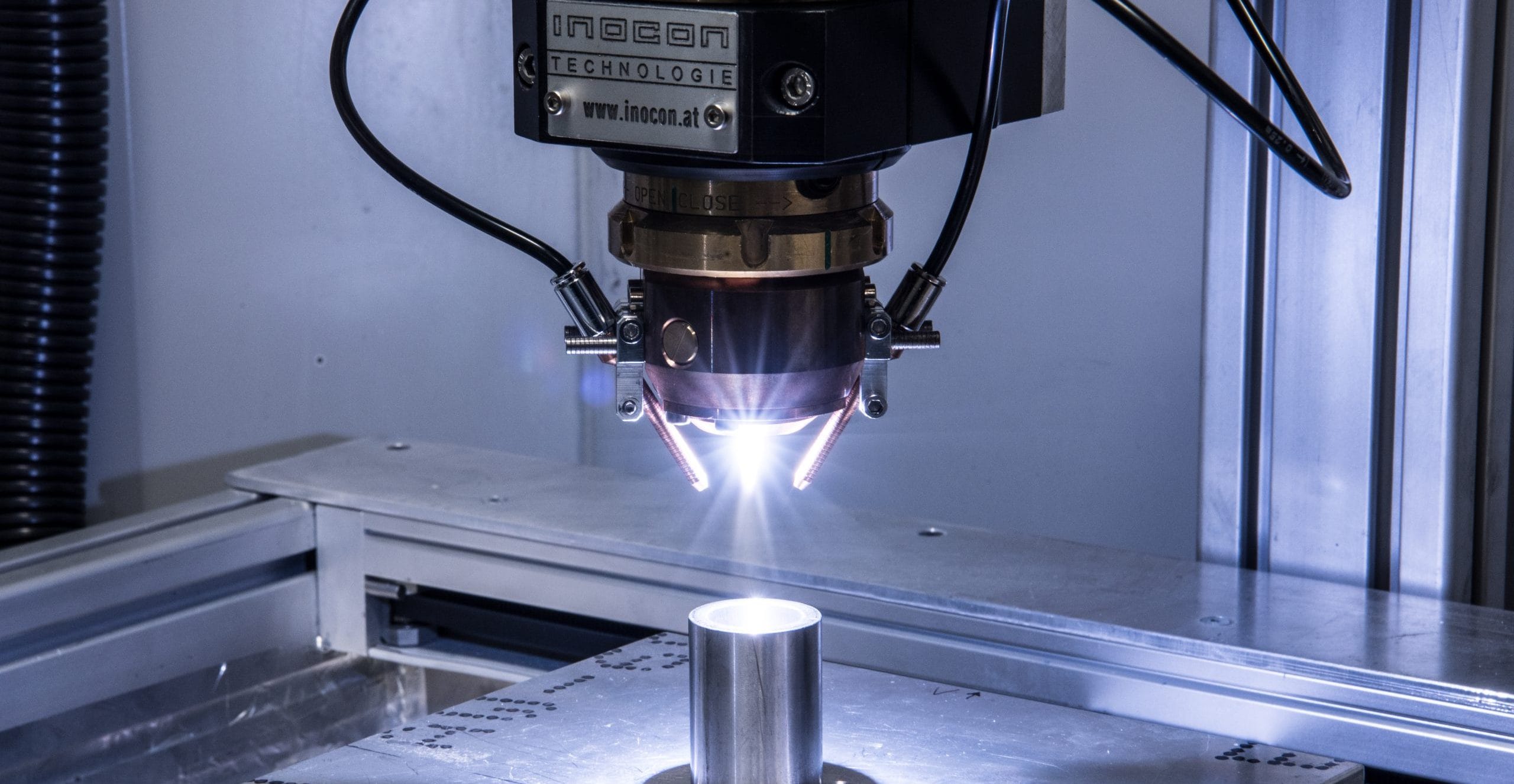
Atmospheric pressure plasma coating technologies (ADPB), e.g. with plasma jets, do not require a vacuum chamber and are therefore subject to hardly any size restrictions with regard to the components to be coated. Possible applications of ADPB include the activation of polymer surfaces by oxygen or inert gas and the deposition of pure metal, oxide and polymer coatings doped with (nano) particles as wear protection, corrosion protection and barrier layers or as biocompatible, antibacterial or biofunctional layers and as electrical insulation layers or conductor tracks and electrodes.
What happens in a low-pressure plasma system?
Low-pressure plasma offers a wide range of surface modification options, e.g. fine cleaning of contaminated components, plasma activation of plastic parts, etching of PTFE or silicon and the coating of plastic and metal parts with PTFE-like layers (see practical example of HMDSO anti-adhesive layer on structured nickel moulding).
What are the advantages of magnetron cathode sputtering?
The advantages of this technology are pore-free, high-purity layers, which are corrosion-reducing or friction-reducing, for example, the deposition of insulators (e.g. aluminium oxide or boron nitride) and semiconductors, low heating of the substrate and relatively high deposition rates of up to 10 nanometres per minute.
Find out more about our services in the area of Functional coatings of components.